
Project Description
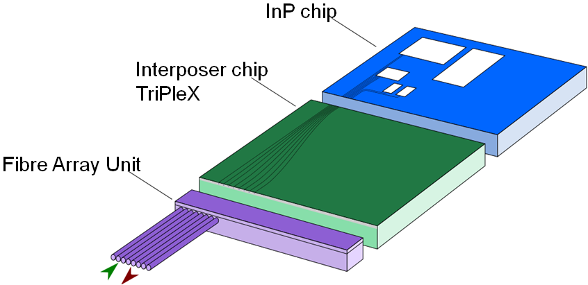
In the figure a simple schematic shows the alignment of three of the main components to be integrated in the hybrid assembly. The waveguide alignment between the TriPlex chip and the InP chip is the most critical requiring alignment accuracy in the range of ±0.1µm.
On-chip alignment of flexible optical waveguide structures will be used to achieve this accuracy in a two stage assembly process which combines passive and active alignment, first a coarse (~1 – 2.0µm) placement by flip chip onto a ceramic carrier, and secondly using the micro-fabricated flexible waveguides, active alignment and then fixing to achieve the final tolerances.
Functionality will be split between the different components, and may depend upon the application requirements. For example the active functions must be on InP – the only platform to provide a building block for optical gain. However, the TriPlex, in addition to hosting the flexible waveguides and actuators can share optical functions based on very low loss dielectric waveguide structures such as splitting and wavelength multiplexing and de-multiplexing. Finally the LTCC carrier (which is maded up of a multi-layer ceramic stack) on which the assembly is carried out, not only provides both a rigid and stable platform for the assembly, but also routes dc electrical and RF signals to the InP chip. PHASTFlex targets a subassembly which is compatible with 25GHz operation , and fibre array (12 ports) optical I/O. The actuators themselves will require additional electrical connections to drive them and desirably the InP chip will contain active circuitry to monitor the alignment (lasers and detectors).
The following figures illustrate this process:
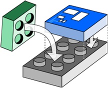
Step 1: Flip-chip assembly onto a carrier
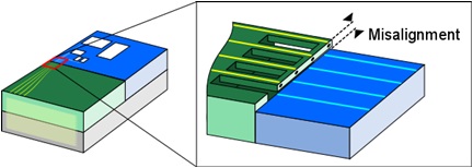
The residual alignment error may have lateral, vertical and rotational components. The longitudinal alignment sensitivity is less stringent being at the µm scale.
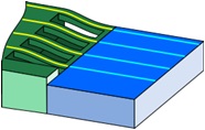
Step 2: The residual alignment error is finally corrected by the use of the flexible guides which may then be fixed using glues, solder or friction.
The activation and fixing of the flexible waveguides is the crucial technology in the project. Many aspects of this scenario push existing technologies to their limits and beyond. It is the task of the PHASTFlex consortium to develop an assembly process flow capable of achieving required alignment accuracy.
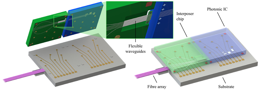
Assembly onto LTCC. The optical interface is shown in the detail box.
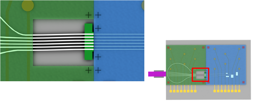
Active alignment and fixing of the waveguides.
Previous page: Welcome to PHASTFlex FP7 EU Project
Next page: Objectives